

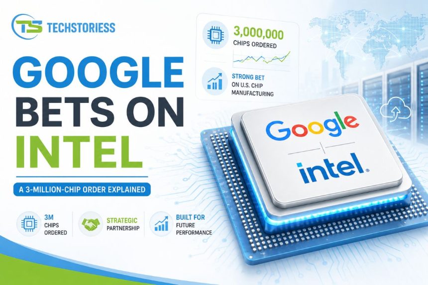
For over a decade, Taiwan was the only destination for the semiconductor industry to procure the world’s most advanced custom silicon which only TSMC can manufacture at scale. However, the landscape shifted in June 2026. That month, Google contracted Intel Foundry to manufacture and package more than 3 million custom Tensor Processing Units to be delivered by 2028. More than just a supplier diversification move, it is the most consequential strategic realignment in the AI hardware industry in the last 10 years – and every infrastructure roadmap built on TSMC’s permanent dominance needs revisiting.
Why Google Stopped Waiting for TSMC
The decision doesn’t reflect a preference for Intel. It reflects capacity constraints: TSMC’s CoWoS – Chip on Wafer on Substrate – is the sophisticated packaging technology that integrates high-bandwidth memory stacks directly to AI processors. This is a crucial enabler for next-generation AI chips to achieve the memory bandwidth that large language model inference demands. CoWoS capacity has been effectively sold out through 2027, locked into long-term contracts with a handful of priority customers. For companies outside that inner tier, the wait means more than delayed shipments; it creates a competitive disadvantage.
Google contracted Intel not because of technical merit, but because TSMC’s queue was closed. This is an important distinction. Intel’s foundry ecosystem has its shortcomings – especially in IP library depth, EDA tool integration, and the multi-customer yield track record that TSMC has built over three decades. Moreover, the experience accumulated over 30 years of serving global fabless semiconductor companies is difficult to replicate in a few years. A single commercial contract, regardless of its volume, does not close that gap.
It also presents an unambiguous strategic lesson for enterprise technology: in a geopolitically volatile world, single-source dependency on any supplier – regardless of technical expertise – is a strategic risk. Headquartered 110 miles from mainland China, TSMC operates under a unique geopolitical shadow. The Taiwan Strait is not a theoretical risk anymore; it is a physical chokepoint through which the majority of the world’s leading-edge semiconductor production flows. Every enterprise that has not formally stress-tested their infrastructure strategy against a Taiwan disruption scenario is accepting catastrophic risk based on outdated assumptions.
How EMIB Packaging Sealed the Deal
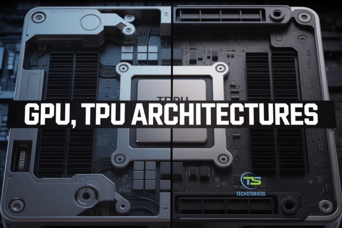
Intel’s 14A introduces RibbonFET Gate-All-Around transistor architecture, wrapping the gate material around all four sides of the transistor channel for complete electrostatic control. GAA geometry provides superior electrostatic control compared to traditional FinFET designs at equivalent process nodes. It directly translates into lower leakage current and higher drive current at the same voltage.
PowerVia, Intel’s backside power delivery network, is the more consequential innovation. Traditional chip design requires power rails and signal routing to compete for the same interconnect layers at the front of the wafer. It increases resistance, voltage drop, and thermal hotspots under heavy load. By moving power delivery entirely to the wafer’s back, PowerVia frees up front-side layers for signal routing. It delivers cleaner signal integrity, reduces voltage drop, and supports higher sustained clock frequencies under the thermal loads generated by weeks of uninterrupted LLM training. For Google’s TPU architecture, which runs at maximum utilization across extended training cycles, this can mean the difference between a chip that maintains peak performance throughout the training cycle and one that throttles under sustained load.
Architectural integration is the major competitive advantage of Intel. RibbonFET, PowerVia, and EMIB together create a full-stack silicon platform that cannot be replicated by pure-play foundries within a single commercial relationship. For hyperscalers that seek performance gains without increasing multi-vendor coordination complexity, that integration delivers procurement efficiency as well as a technical advantage.
Intel 14A offers a complete Transistor-to-Packaging architecture – a full-stack commitment. Intel’s Embedded Multi-die Interconnect Bridge gave Google a cost-efficient, high-density chiplet integration platform unconstrained by the reticle size limits that restrict CoWoS scaling at its largest configurations. It delivered where TSMC’s interposer approach could not – at equivalent scale.
TSMC’s CoWoS employs a large silicon interposer that spans the entire package footprint, maximizing effective bandwidth density. However, interposer size is constrained by reticle limits, expanding the physical footprint of the integrated system, and aggressively compressing costs as interposer area scales. Intel’s EMIB deploys small bridge chips only at the precise die-to-die interface points where high-bandwidth communication is required. Such targeted architecture reduces cost at scale, allows more flexible die placement, and maintains competitive bandwidth density without inheriting CoWoS’s scaling constraints.
A practical, production-ready HBM4 interface was the critical differentiator. HBM4’s shift from passive to active logic bases enables memory bandwidth throughput that could not be sustained with prior generations. Realizing that bandwidth in production demands a substrate routing thousands of parallel signal lines at extremely tight pitch between memory and compute. EMIB delivers precisely that capability – outside the CoWoS capacity queue that has been constraining Google’s TPU roadmap for two years.
The Geopolitics of Domestic Silicon
Beyond the engineering and manufacturing details, the Google–Intel partnership tells a much bigger story. The US CHIPS and Science Act committed tens of billions of dollars to create the commercially viable conditions for exactly this kind of high-volume manufacturing contract. Policymakers didn’t want the future of global AI infrastructure to depend on a single geopolitically sensitive manufacturing hub. Google’s order for over 3 million TPUs doesn’t merely validate government policy; it signals corporate strategy.
The CHIPS Act advantage is durable and structural. More than merely a geopolitical hedge, Intel’s domestic manufacturing posture is a procurement moat in a regulatory environment that increasingly prioritizes supply chain provenance. Similar CoWoS constraints also affect Microsoft, Amazon, and Meta. By executing successfully on Google’s contract with Intel, the company will approach the next hyperscaler conversation from a position of proven execution rather than promise.
The EU AI Act requires providers of high-risk AI systems to maintain comprehensive technical documentation, implement risk management processes, and ensure an appropriate level of cybersecurity throughout the AI system’s lifecycle. Meanwhile, U.S. government policies continue to strengthen and promote trusted semiconductor supply chains for critical AI infrastructure. Together, these developments are elevating the importance of hardware traceability, manufacturing assurance, and supply-chain transparency in procurement decisions, even if they are not explicit statutory requirements. Google’s U.S.-manufactured TPUs therefore are well positioned for organizations that prioritize trusted manufacturing and resilient supply chains. In the foreseeable future, these considerations are likely to carry increasing weight for enterprises operating in regulated sectors.
The Foundry Equation Is Being Rewritten – But the Real Test Is Still Ahead
Google’s multi-million-unit commitment offers Intel the commercial credibility to compete for additional hyperscaler partnerships, which will eventually strengthen its position as a leading-edge foundry. With more leading cloud providers gaining access to a viable alternative at the cutting edge, it will intensify competition, thus improving pricing dynamics, extending available manufacturing capacity, and accelerating innovation across the AI infrastructure ecosystem. In the foreseeable future, it will help erode the scarcity premium historically associated with TSMC’s leading-edge manufacturing.
In reality, the ultimate challenge is execution, and Intel’s foundry history still casts a long shadow, which cannot be erased by a single contract. Securing an ambitious contract is one thing; delivering 3 million TPUs by 2028 at competitive yield rates is the real test for a foundry business still rebuilding credibility after years of process delays. Moreover, Intel must navigate a strategic tension: unlike TSMC, which operates as a pure-play foundry, Intel designs and manufactures its own AI accelerators while simultaneously pitching hyperscalers as a foundry partner. It creates a perceived conflict of interest, and managing it transparently will be as important as the silicon itself.
The Google contract is not a verdict but an audition. How Intel delivers at scale will determine whether the foundry map gets redrawn – or quietly rolled back up.


