

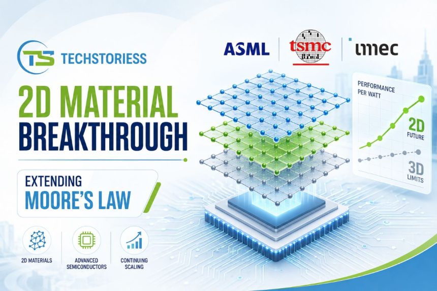
At the 2026 IEEE/JSAP Symposium on VLSI Technology and Circuits in Honolulu, a research coalition comprising nanoelectronics pioneer imec, Dutch lithography giant ASML, and contract chip manufacturing leader TSMC, unveiled a landmark technological breakthrough. The coalition demonstrated a scalable 300mm (wafer-sized) integration approach for two-dimensional (2D) material transistors, achieving a 50nm contacted poly pitch (the minimum spacing between transistor gates on a chip) with 94% of integrated transistors switching correctly and an on/off current ratio exceeding 100,000. The achievement marks a world first.
The 94% yield may be the most significant achievement. Academic labs routinely produce a single flawless “hero device” while 99 neighboring transistors fail. Using a single EUV (precision laser-based) exposure, the trio fabricated channel lengths as short as 28 nm, trimming active widths to 75 nm and an equivalent oxide thickness (the insulating layer thickness) below 2 nm.
Why Silicon Has Hit Its Physical Limit
Trimming silicon transistor channels to fewer than 50 atoms across pushes conventional switching into the realm of quantum mechanics. Electrons are no longer fully blocked by the closed gate but pass directly through it. This phenomenon, known as quantum tunneling, causes leakage current, heat buildup, and rising power consumption per transistor.
The solution lies in a class of materials called Transition Metal Dichalcogenides (TMDs)-specifically Molybdenum Disulfide (MoS₂), Tungsten Disulfide (WS₂), and Tungsten Diselenide (WSe₂). Owing to their atomically thin structure, they can efficiently control electrical current while maintaining charge carrier mobility (the speed at which electrical signals move through the material) at extremely small dimensions. This makes them promising candidates for future logic scaling. The structural perfection of the channel at the atomic level allows the gate to more effectively shut down electron flow, thereby significantly reducing the leakage problem that plagues silicon at sub-5nm nodes.
The joint demonstration used WSe₂ channels and achieved very low off-current (Ioff), the power that leaks even when a transistor is switched off, at zero gate voltage for both n-type and p-type transistors (the two complementary transistor polarities required to build any functional chip circuit), approaching the performance of record-setting laboratory devices, particularly for pFETs. That latter result holds special significance. It addresses a more than decade-long challenge in the field-achieving high-performance p-type transistors in 2D materials, a prerequisite for building functional CMOS (the standard chip architecture that pairs both transistor types to minimize power consumption) logic circuits.
Three Engineering Breakthroughs Hidden Inside One Announcement
The imec-ASML-TSMC result isn’t a single insight. It simultaneously solved three distinct engineering problems – if any one had remained unsolved, it would have kept 2D transistors trapped in academic papers. Each breakthrough addressed a specific limitation that had blocked the field for many years.
The Architecture Inversion
Several prior attempts failed because they required depositing metal onto fragile 2D films after the channel was in place, resulting in thermal damage. Instead, the team began by patterning tungsten-filled contact trenches (the microscopic metal connectors that link transistors to the rest of the circuit), then transferred the 2D channel on top, with the gate deposited afterward. Termed a “reverse” thin-film-transistor (TFT) flow by imec, this approach enabled the resulting bottom-contact geometry (a configuration where electrical contacts sit beneath the active material rather than on top), which is responsible for the clean off-state behavior in which both transistor polarities stop conducting at zero gate voltage.
The CMOS Parity Problem – Solved
While it was already possible to fabricate nFETs from MoS₂, there still remained a crucial barrier: matching them with reliable pFETs on the same wafer-a prerequisite for real CMOS logic circuits. The process flow demonstrated here can be applied to 2D channel materials beyond MoS₂, WS₂, and WSe₂, underscoring the flexibility of the process and its potential compatibility with future 2D material systems.
EUV as the Precision Instrument
Etienne De Poortere, ASML’s Director of Technology Development Centre Europe, explained that using EUV (extreme ultraviolet) lithography enabled the team to achieve finer dimensions than previous demonstrations, collapsing the gate pitch to 50 nm while keeping contact resistance (the electrical friction at the junction between metal and semiconductor) low enough to preserve transistor performance. Previous 2D material research largely relied on older-generation lithography tools. The use of single-patterning EUV delivered the precision required to achieve these dimensions.
The Signal Most Analysts Are Missing: The BEOL Insertion Strategy
This is the strategic move. Here, the technology does not compete directly with silicon at the most demanding compute layer, but positions 2D transistors as power-management infrastructure integrated into layers above and below the primary logic stack (the core silicon transistor tiers where computation happens). A proprietary low-temperature BEOL (back-end-of-line: the manufacturing stage where circuits are connected with metal wiring after transistors are built) process has already been developed by a startup called CDimension, enabling the direct growth of atomically thin MoS₂ films onto silicon substrates, and the company is quietly working with multiple chipmakers to integrate 2D devices without disturbing existing front-end silicon flows (the earlier fabrication stages where the transistors themselves are formed).
The Supply Chain Nobody Is Watching Yet
One of the most significant yet least discussed dimensions of this narrative is the materials supply chain. Phoenix-based mining company Freeport-McMoRan is the leading producer of molybdenum chemicals, including molybdenum disulfide (MoS₂), in the United States. Federal investment in 2D-material semiconductor research across U.S. national laboratories is also accelerating, steadily increasing demand for high-purity crystals. Presently, the semiconductor-grade MoS₂ crystal market is valued in the low tens of millions of dollars annually. However, if 2D transistors evolve from laboratory-scale demonstrations to commercial manufacturing-even initially for back-end-of-line (BEOL) power management applications, before high-performance logic devices-the demand for ultra-high-purity transition metal dichalcogenide (TMD) feedstocks (the raw material inputs refined to atomic-level purity for chip fabrication) is likely to rise sharply worldwide.
The semiconductor industry has already experienced how vulnerable it can become to supply constraints involving critical materials such as rare earth elements, helium, and high-purity neon gas during the Ukraine conflict. Another materials bottleneck may be around the corner, though it is not yet widely recognized-and no, it is not gallium or germanium. The next constraint that is quietly emerging is the availability of semiconductor-grade molybdenum and tungsten crystals, which are not yet produced at commercial scale by any supplier at the time of writing.
The Geopolitical Chessboard
The 94% yield number is not just an engineering milestone but a strategic signal for China’s semiconductor ecosystem. The Western-Taiwanese consortium of imec, ASML, and TSMC has collectively demonstrated a robust, manufacturable, and scalable integration route requiring precisely the EUV tooling that cannot be accessed by China under current export controls. Without access to ASML’s High-NA and standard EUV systems (the most advanced chipmaking machines in existence), Chinese foundries have increasingly pursued architectural solutions-such as stacking older-generation transistors to approximate advanced-node performance without depending on the most advanced lithography. While that approach has demonstrated meaningful progress and should not be underestimated, it faces a fundamentally different ceiling.
What Comes Next, and When
TSMC’s roadmap places 2D FET (field-effect transistor, the fundamental switching unit in modern chips) technology at the A2 (0.2nm) node, with the first high-volume application expected around 2043, following an intermediate A7 (0.7nm) node featuring BEOL-integrated 2D devices. However, commercial sub-1nm nodes incorporating 2D materials will begin emerging during the 2030s.
But the BEOL timeline is far more immediate. According to imec’s A7 node roadmap, 2D TMD devices could enter production wafers as power management components before the decade ends-not as the primary logic transistor technology, but as the switch supporting the transistor you compute on. That distinction is crucial for investors, procurement teams, and supply chain planners assessing the technology’s near-term commercial potential.
The gap between physics experiment and manufacturing has now been substantially narrowed, at 94% yield, on a 300mm wafer, with EUV lithography already deployed across TSMC fabs worldwide. The current challenge is the harder, gradual, more consequential work of turning a laboratory breakthrough into a commercially viable supply chain.


